Norcada TEM Window Arrays Enable Multiple In-Situ Analysis
March 02, 2009 (PRLEAP.COM) Business News
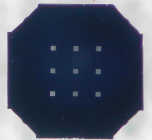
EDMONTON, ALBERTA - March 2, 2009 Norcada Inc., a MEMS design and product development company, announced today the availability of a new TEM nitride window array device to the TEM research community. The new TEM window array devices enable the end users to conduct multiple analyses in-situ on a single TEM nitride membrane device, which increases the throughput significantly.The TA301 series TEM nitride window array device (see photo on left) has nine individual membrane windows in a 3x3 array pattern on a single 200µm thickness silicon frame. The silicon frame is octagon shaped and fits inside a 3mm diameter circle. Each silicon nitride window of the 3x3 array is 100µm by 100µm in size, and the spacing between two adjacent windows is 350µm (edge to edge).
"We use the TEM window arrays from Norcada in our investigation of amorphous silicon and germanium crystallization process using dynamic TEM imaging method with nanosecond temporal resolution," said Ms. Liliya Nikolova and Professor Federico Rosei at INRS of Quebec. "The TEM window arrays allow us to carry out multiple experiments in-situ on a single TEM window array device which reduces the TEM sample preparation time and increases our throughout significantly."
"We are very pleased with the positive impact our new TEM window array devices are having for our customers," said Yuebin Ning, Vice President Research & Development of Norcada. "The addition of the TEM window arrays further complements our product offerings in the area of TEM silicon nitride windows for TEM Analysis studies."
The initial devices being offered have a 100nm thickness low stress silicon nitride membrane (part number TA301C). Additional TEM devices with 30nm and 50nm thickness silicon nitride membranes will become available shortly.
About Norcada Inc.
Norcada is a MEMS (Micro-Electro-Mechanical-System) product development company, with extensive industrial experience and capabilities in MEMS design and fabrication for sensors, X-ray and TEM analysis windows, and other commercial devices. Founded in 2001, Norcada has a state-of-the-art MEMS design, prototyping, and test facility in Edmonton, Canada, which is home to one of the largest micro and nano technology clusters in North America. Norcada offers a wide range of MEMS products including standard silicon and nitride membrane windows for the TEM microscopy and X-ray spectroscopy research community, silicon optical benches and MEMS mirrors for the telecom industry.
